
Two Compute Nodes: Physical vs. Virtual
The Gigawatt Machine: NVIDIA, Google, and the Engineering of Scale 5/12

1. Introduction
In the previous articles, we examined the silicon engines (Article 2), the density strategies (Article 3), and the software ecosystems (Article 4) that power AI supercomputers. Now we turn to the fundamental question: What is the atomic unit of computation?
For the last decade, the industry agreed on a definition: a “node” was a discrete, physical server chassis housing 8 GPUs. This “supercomputer-in-a-box” (like the NVIDIA DGX) was the standard building block. You connected thousands of these nodes with high-speed networking to build a cluster.
However, as we enter the Gigawatt era,the definition of the “compute node” has bifurcated into two contrasting philosophies, each driven by the architectural choices we explored in Article 1:
Path A (NVIDIA): The Physical Evolution. The node is getting bigger. NVIDIA has evolved from a server-scale node (8 GPUs) to a rack-scale node (72+ GPUs), turning the entire cabinet into a single, liquid-cooled monolith. The strategy is to compress maximum compute into a defined physical volume.
Path B (Google): The Virtual Evolution. The node is disappearing. Google has abstracted away the physical hardware, treating the “node” as a virtual entry point into a massive, flat mesh of TPUs. The strategy is to make the physical packaging irrelevant so the fabric can grow without bounds.
This article deconstructs how the physics of copper, cooling, and fabric have driven NVIDIA to build bigger boxes, while Google has made the box disappear entirely.
2. The NVIDIA Path: Physical Scale-Up
NVIDIA’s philosophy is rooted in density. To make models run faster, compress the compute into the smallest possible physical space. This has driven a two-phase evolution: from the server to the rack.
Phase 1: The Server-Scale Node (DGX B200)
For enterprise deployments and standard clusters, the atomic unit is the 8-GPU server. The DGX B200 represents the current instantiation of this design philosophy—the most powerful air-cooled system in a server footprint.
Why 8 GPUs? The Engineering Limits
The number 8 results from two hard physical constraints:
The Copper Limit: At NVLink speeds (1.8 TB/s bidirectional), electrical signals degrade rapidly. The 8-GPU chassis is the maximum size where you can connect all chips via passive copper traces on a motherboard without signal integrity issues.
Switch Radix: Eight GPUs saturate the port count of the internal NVSwitch chips. Adding a 9th GPU would break the non-blocking fabric architecture.
The Internal Fabric: A Single NVLink Domain
Inside the DGX B200, the 8 GPUs function as one unified system:
GPU-to-GPU (East-West): 18 NVLink 5.0 connections per GPU provide 1.8 TB/s of bidirectional bandwidth. This switching happens entirely inside the box.
CPU-to-GPU (North-South): The system uses the GB200 Superchip, replacing legacy PCIe with NVLink-C2C. This fuses the Grace CPU and Blackwell GPU into a single memory space, allowing GPUs to access the 960GB of LPDDR5X system memory as their own.
The Thermal Wall: Pushing Air Cooling to Its Limit
Form Factor: The DGX B200 expanded from 8U (DGX H100) to 10U to accommodate larger heatsinks.
Power Draw: 14.3 kW—a 40% increase over the 10.2 kW DGX H100.
Deployment Challenge: At this power density, operators must leave empty rack slots to prevent “hot spots,” and fans scream at 10,000+ RPM.
The DGX B200 delivers 144 PetaFLOPS (FP8) per node, but it represents the absolute limit of what air cooling can achieve.
Phase 2: The Rack-Scale Node (GB200 NVL72)
To break the 8-GPU limit, NVIDIA redefined the physical boundaries of the node. The node is no longer a server; the node is the entire rack.
The Monolith: 72 GPUs as One Computer
The GB200 NVL72 is a 120 kW, liquid-cooled, 42U rack. It is not a collection of servers—it’s a single computer:
The Architecture: 72 B200 GPUs and 36 Grace CPUs are hard-wired together with a massive copper backplane (the “spine”) that runs vertically through the cabinet.
The Copper Advantage: Because the GPUs are stacked vertically in one cabinet, NVIDIA can connect all 72 using passive copper cabling. This avoids power-hungry optical transceivers, saving approximately 20kW per rack.
Unified Memory: The entire system functions as one giant accelerator with 31 TB of unified memory (13.8 TB HBM3e + 17.3 TB LPDDR5X).
Performance: The Generational Leap
The evolution from Hopper through Blackwell and into the roadmapped Vera Rubin platforms reveals the trajectory of rack-scale computing:
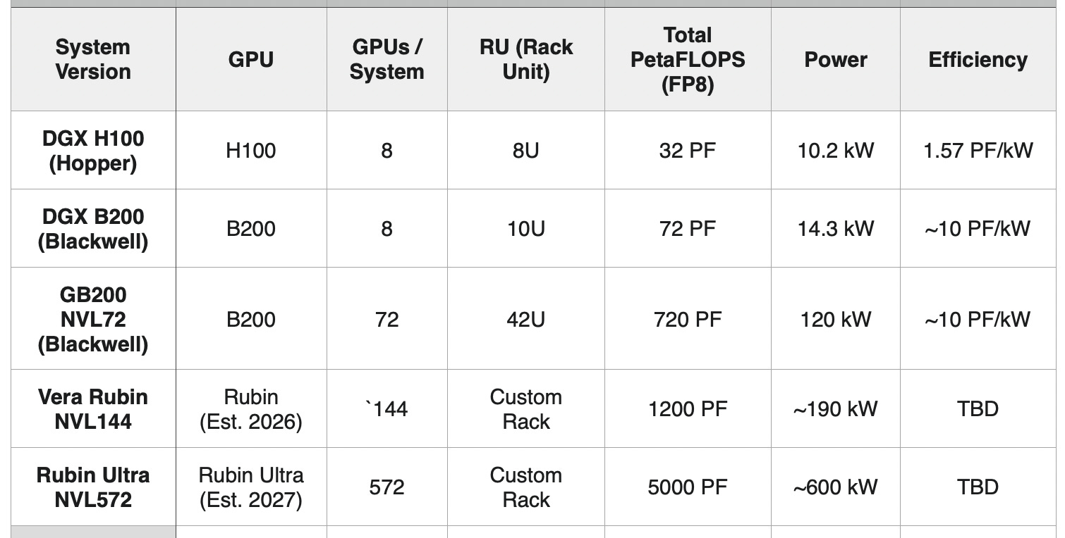
The GB200 NVL72 achieves 81x the raw compute of the DGX H100, while simultaneously improving power efficiency by 6.4x (from ~1.57 to ~10 PetaFLOPS per kilowatt). The roadmap shows NVIDIA’s commitment to continuing this rack-scale expansion, with the Vera Rubin Ultra NVL572 targeting nearly 4x the performance of today’s GB200 NVL72.
Liquid Cooling: The Infrastructure Mandate
At 120 kW per rack, air cooling is physically impossible. The GB200 NVL72 uses direct-to-chip (DTC) liquid cooling, where cold plates are mounted on every GPU and CPU:
Water Requirement: Standard facility water (inlet temperature up to 25°C / 77°F).
Infrastructure Impact: Data centers must install industrial-scale hydraulic systems, circulating millions of gallons of coolant.
As rack-scale nodes continue to grow (144 GPUs, then 572 GPUs), the power density and cooling requirements will intensify further, driving data centers toward becoming industrial power plants with integrated hydraulic infrastructure.
The Network: Pushing the Bottleneck
The critical innovation is where the “cluster” begins:
DGX B200 (Server-Scale): The cluster begins immediately outside the 8-GPU chassis. Even communication between servers in the same rack must traverse the external InfiniBand network (800 Gb/s).
GB200 NVL72 (Rack-Scale): The cluster begins only when connecting one rack to another. All 72 GPUs communicate over the internal NVLink fabric, avoiding the external network entirely. This pushes the network bottleneck from every 8 GPUs to every 72 GPUs—a 9x reduction in inter-node traffic.
Scaling Further: The Multi-Generation Roadmap
The GB200 NVL72 is not the endpoint of NVIDIA’s rack-scale vision. Using the 5th-generation and future NVLink Switch Systems, NVIDIA is systematically expanding the maximum size of a single NVLink Domain:
Today - Blackwell (2024-2025):
GB200 NVL72: 72 GPUs in a single rack
GB200 NVL72 Pods: Up to 8 racks = 576 GPUs in one continuous NVLink Domain
Near Future - Vera Rubin (2026):
Rubin NVL144: 144 GPUs in a multi-rack configuration
This effectively doubles the size of the rack-scale node, allowing massive models to remain within a single, high-speed memory space without crossing into slower inter-rack networking.
Far Future - Vera Rubin Ultra (2027):
Rubin Ultra NVL572: 572 GPUs in a single NVLink Domain
At this scale, the “Super-Node” effectively becomes a small supercomputer, with nearly 600 GPUs addressable as one giant, coherently-cached brain.
The 5,000 PetaFLOPS of compute in a single domain approaches the entire computational capacity of early supercomputing facilities.
This roadmap reveals NVIDIA’s long-term strategy: expand the physical node to encompass what was once an entire cluster. By 2027, the rack-scale node will be 8x larger than today (572 vs 72 GPUs), effectively turning multiple aisles of racks into one massive, unified logic gate.
Implication: The “network bottleneck” that limits distributed training will be pushed from every 72 GPUs (today) to every 572 GPUs (2027)—nearly eliminating it for most trillion-parameter model training workloads.
3. The Google Path: Virtual Scale-Out
Google’s philosophy is rooted in fabric scale. They prioritize the size of the network over the density of the box. Consequently, their “node” story is not about building a bigger box, but about making the box irrelevant so the matrix can grow.
The “Invisible” Physical Node
If you walked into a Google data center and pulled out a TPU server tray, you would hold a relatively modest piece of hardware: a standard-sized board with 4 or 8 TPU chips.
Unlike the NVIDIA DGX, this physical node is architecturally transparent:
No Local Switch: There is no equivalent to NVSwitch inside the tray.
Passthrough Design: Every single TPU chip has optical ports that bypass the board and connect directly to the massive data center fabric (the Optical Circuit Switches).
The philosophy: The physical server tray is just a holder for the silicon. The software treats the tray as a simple socket.
The Virtual Node: The TPU Pod
Because the physical node is abstracted, the “Atomic Unit” for a Google engineer becomes the TPU Pod—a massive, flat mesh of thousands of chips.
Scaling the Matrix
Instead of building denser racks (Scale-Up), Google scales by adding more TPUs to the flat fabric (Scale-Out):
TPU v4 Pod: 4,096 chips in a 3D Torus mesh
TPU v5p Pod: 8,960 chips in a 3D Torus mesh
TPU v7 “Ironwood”: 9,216 chips
This represents a Pod size 16x larger than NVIDIA’s current maximum NVLink domain (576 GPUs in a GB200 NVL72 Pod).
However, with NVIDIA’s roadmap targeting 572 GPUs in a single Rubin Ultra NVL572 domain, the gap is narrowing—NVIDIA is converging on Google’s Pod-scale integration through the inverse path of extreme rack-scale density.
The Interconnect: ICI (Inter-Chip Interconnect)
This virtual node relies on Google’s proprietary ICI fabric:
Bandwidth: Each TPU v5p has 600 GB/s of ICI bandwidth (compared to NVIDIA’s 1.8 TB/s).
Topology: These links connect each chip directly to its 6 neighbors in the mesh (north, south, east, west, up, down).
The Trade-off: Google accepts lower per-chip bandwidth in exchange for a massive, flat fabric that requires no hierarchy.
The Optical Circuit Switch (OCS): The Physical Fabric
Unlike NVIDIA’s electrical NVLink switches, Google’s ICI relies on Optical Circuit Switching (OCS)—a fundamentally different networking technology:
Physical Mechanism: The OCS uses arrays of tiny, steerable mirrors (MEMS mirrors) to redirect beams of light. Each mirror can physically rotate to point a laser beam from any input fiber to any output fiber, creating a direct optical path between two TPU chips.
Circuit-Switched Architecture: Unlike traditional packet-switched networks (like InfiniBand), the OCS does not forward packets. Instead, it establishes dedicated optical circuits—direct “light pipes” between TPU pairs. Once a circuit is established, data flows at full speed with zero switching overhead.
Static Topology: The 3D Torus topology is programmed into the OCS at the start of a training job. The mirrors are set to specific angles, creating the mesh pattern, and they remain in that configuration for the duration of the workload. This is why Google’s approach is called “deterministic”—the network topology is fixed and known in advance.
The Reconfiguration Trade-off: Physically rotating MEMS mirrors takes milliseconds—far too slow for dynamic packet routing. However, because AI training workloads are predictable and long-running (days to weeks), this static topology is ideal. The XLA compiler knows the exact mesh structure and schedules all data movement accordingly.
This is the critical innovation that enables Google’s “virtual node” concept: the physical server tray is irrelevant because every TPU is directly connected to every other TPU through pre-configured optical paths. There is no hierarchy, no switch hops, no routing decisions—just dedicated optical circuits forming a massive, flat mesh.
Why Lower Bandwidth Works
At first glance, 600 GB/s (TPU) versus 1.8 TB/s (GPU) seems like a massive disadvantage. However, the OCS architecture delivers advantages that offset the lower per-chip bandwidth:
Uniform Distance: In a 3D Torus, every chip is equidistant from every other chip (in terms of network hops). There are no “fast” chips and “slow” chips. Every TPU is exactly 6 optical hops from any other TPU, creating predictable latency.
Zero Switch Overhead: Because the OCS establishes dedicated optical circuits, there is no packet switching, no routing lookups, no buffer management, and no congestion control. The full 600 GB/s bandwidth is available without protocol overhead.
Deterministic Routing: Because the topology is fixed and known at compile time, XLA can schedule data movement with perfect precision, eliminating congestion. The compiler calculates the exact nanosecond when each data transfer will occur, ensuring no two transfers ever collide on the same optical path.
Scale Advantage: The ability to keep 9,216 chips in a single domain means that massive workloads never leave the optical fabric—they don’t hit the slower Tier-2 network that even NVIDIA’s largest future clusters will require beyond 572 GPUs.
The result: Google’s lower per-chip bandwidth delivers higher effective utilization because the OCS eliminates the inefficiencies of packet-switched networks.
4. Liquid Cooling the Chip
While NVIDIA positioned liquid cooling as a recent breakthrough necessary for the Blackwell generation, Google has been using liquid cooling in production data centers since 2017. However, their approach differs significantly from NVIDIA’s integrated rack-scale design.
TPU v2/v3 (2017-2018): The Liquid Cooling Transition
With TPU v2, Google adopted liquid cooling at the board level—each TPU server tray includes integrated cold plates, but unlike NVIDIA’s GB200 NVL72, the cooling infrastructure is not monolithically integrated into the rack. The TPU trays remain modular with quick-disconnect fittings for coolant lines, while cooling distribution units (CDUs) are rack-mounted but separate from compute trays.
TPU v4/v5p/v7 (2021-Present): Advanced Liquid Cooling
The current generation continues with liquid cooling at higher power densities. TPU v5p chips consume approximately 275W, while TPU v7 “Ironwood” is estimated at 400-600W per chip given its 10x performance leap.
The Key Difference: Modular vs. Monolithic
The fundamental distinction reflects their broader architectural strategies:
Google’s Approach (Modular):
Each TPU tray is an independent, liquid-cooled unit with quick-disconnect fittings
Rack is just a physical shelf; cooling infrastructure is separate from compute hardware
Failed trays can be hot-swapped without draining the rack
Philosophy: Liquid cooling is a utility provided by data center infrastructure
NVIDIA’s Approach (Integrated):
GB200 NVL72: Cooling system built directly into the 42U rack
Entire rack ships as one pre-integrated unit with coolant distribution, pumps, and manifolds
Philosophy: Liquid cooling is part of the product
5. The Engineering Trade-offs
NVIDIA: Granularity and Modularity (The Rack-Scale Node)
The NVL72 / NVL144 / NVL576 architectures prioritize Composable Scale. Even though the “node” has grown from a server to a rack (or row), it remains a flexible building block.
Elastic Deployment: A data center can deploy a single GB200 NVL72 (72 GPUs) for inference, or connect eight of them into a Rubin Ultra NVL576 (576 GPUs) for training. You are not forced to deploy a warehouse-sized mesh to get started.
Physical Segmentation: The system respects physical boundaries. A 72-GPU rack is a discrete thermal and power domain. If one rack fails or needs maintenance, it can be isolated without destabilizing a 10,000-chip cluster.
Multi-Tenancy: This architecture is ideal for cloud providers who need to serve diverse workloads—allocating one rack to Team A for Llama 3 training, and another to Team B for Claude inference.
Verdict: Ideal for Enterprise AI and Cloud, where flexibility and incremental scaling are critical.
Google: Integration and Unity (The TPU Pod)
The TPU Pod architecture prioritizes Maximum Integration. It treats the entire warehouse as a single device.
The “Zero-Boundary” Fabric: In a 9,216-chip Ironwood Pod, the workload stays entirely within the optical ICI fabric. There is no “performance cliff” every 72 or 576 chips; the mesh is continuous.
Simplified Programming: To the XLA compiler, the Pod looks like one giant 9,000-core processor. Developers don’t need to manually partition the model across separate racks; the compiler handles the data flow across the entire mesh.
Stability via Rigidity: Because the topology is fixed and uniform, the system is less flexible but more predictable. A broken chip is treated as a “bad sector” on a hard drive—mapped out by software without disrupting the massive job.
Verdict: Ideal for Frontier Model Training (Gemini, Claude), where a single massive workload monopolizes the entire cluster for months.
The Convergence
Interestingly, both approaches are converging toward similar goals through different paths, now that both companies are doing their version of both scaling up and scaling out:
NVIDIA: The GB200 NVL72 effectively creates a “mini-Pod” of 72 GPUs. By 2027, the Rubin Ultra NVL576 will expand this to 576 GPUs—closing the gap with Google’s integration. It mimics the TPU Pod’s unity but retains the rack-based modularity.
Google: The TPU v7 “Ironwood” represents a 10x leap in per-chip performance. By chasing NVIDIA-class density, Google is reducing the number of chips needed to do the same work, effectively making their massive mesh more potent per square meter.
The Key Difference: From a networking perspective, NVIDIA’s approach remains Modular (the Rack is the unit), while Google’s approach remains Monolithic (the Pod is the unit).
5. Conclusion: Two Definitions of the Node
The “compute node” has bifurcated to meet different strategic goals:
NVIDIA defines the node by physics. They compress more power into a defined physical volume (Server → Rack → Multi-Rack), using copper and liquid cooling to maximize density. The result is the Super-Node:
Today: GB200 NVL72 (72 GPUs, 31 TB unified memory)
2026: Vera Rubin NVL144 (144 GPUs)
2027: Vera Rubin Ultra NVL572 (572 GPUs, 5,000 PetaFLOPS)
Google defines the node by fabric. They expand the network to encompass more chips, rendering the physical packaging architecturally irrelevant. The result is the Super-Matrix (TPU Pod)—a 9,216-chip optical mesh where every chip is equidistant from every other.
Both philosophies solve the same problem—training trillion-parameter models—through inverse strategies:
NVIDIA says: “Build ultra-dense islands, then connect them.”
Google says: “Build a massive, seamless fabric that eliminates the islands.”
By 2027, NVIDIA’s largest “island” (Vera Rubin Ultra NVL572 with 572 GPUs) will approach the scale of a small supercomputer, while Google’s “fabric” will continue to seamlessly connect over 9,000 chips. The two approaches will still differ in granularity and deployment philosophy, but both will deliver multi-exaFLOP capability within a single coherent memory domain.
Regardless of whether the node is a physical monolith or a virtual matrix, these massive systems share a common vulnerability: they are composed of millions of parts, and parts break.
In the next article, “Article 6: Two Network Topologies,” we will examine how NVIDIA’s hierarchical NVLink fabric and Google’s flat ICI mesh handle the physics of data movement at gigawatt scale.
Outstanding anlysis of the node abstraction wars. The optical circuit switch detail is what makes Google's approach actually viable at this scale becuase those MEMS mirrors sidestep packet-switching latency entirely. What's underrated though is how the static topology requirement becomes a compielr advantage rather than a limitation.