
Two Silicon Foundations for Scale
The Gigawatt Machine: NVIDIA, Google, and the Engineering of Scale 2/12

1. Introduction
To build a machine capable of training a trillion-parameter models, you need silicon designed for one specific purpose: massive, parallel matrix multiplication, collectively known as AI Accelerators.
While the industry often uses “GPU” as a catch-all term for these chips, the reality is a tale of two distinct lineages. To understand the Gigawatt Machine, we must trace the evolution of the two dominant families that power it:
The GPU (NVIDIA): A flexible, general-purpose parallel processor that evolved from rendering video games to training AI.
The TPU (Google): A specialized, domain-specific ASIC (Application-Specific Integrated Circuit) built from a blank sheet of paper to optimize matrix math.
This article traces the architectural history of these two families, defining the vocabulary—Tensor Cores, HBM, and Systolic Arrays—that you will need to understand the engineering deep dives in the rest of this series.
2. Key Performance Definitions
Regardless of the architecture (GPU or TPU), three metrics define the power of an accelerator. We will reference these throughout the series:
1. FLOPS (Compute) How much math the chip can do per second.
Example (NVIDIA B200): Delivers ~4,500 TeraFLOPS (FP8).
Example (Google TPU v7): Delivers ~4,614 TeraFLOPS (FP8).
Note how closely matched these two engines are when running the same 8-bit math.
2. HBM (Memory Capacity) How big a model fits on the chip.
Example (NVIDIA B200): Packs 192 GB of HBM3e.
Example (Google TPU v7): Matches this with 192 GB of HBM3e.
Why it matters: If the model doesn’t fit in HBM, it must be split across chips. Since both chips have the same capacity, they can hold the same size model slices, making the network the deciding factor for performance.
3. Memory Bandwidth (Speed) How fast data moves from memory to the compute cores.
Example (NVIDIA B200): 8 TB/s.
Example (Google TPU v7): ~7.4 TB/s.
Why it matters: This is often the true bottleneck in AI training. A fast chip with slow memory spends most of its time idling.
3. Evolution to Lower Precision
In traditional High-Performance Computing (like weather simulation), precision is everything (64-bit). In AI, the rules are inverted. Neural networks are surprisingly resilient to noise; they do not need 7 decimal places to decide if an image is a “Cat.” They just need “directional accuracy.”
By using fewer bits to represent a number (Quantization), we gain two massive advantages:
Memory Bandwidth: Sending a 4-bit number moves 8x faster over the wire than a 32-bit number.
Compute Density: You can pack 4x as many 4-bit calculators into the same silicon area.
4. The NVIDIA GPU: The “Simultaneous” Machine
The NVIDIA GPU architecture is defined by SIMT (Single Instruction, Multiple Threads).
In a traditional CPU (Sequential Processing), one core executes one instruction on one piece of data at a time. In a GPU, a single instruction controller drives thousands of cores simultaneously.
The Mechanism: The GPU groups threads into bundles that execute in lockstep. A single instruction drives thousands of active data lanes simultaneously, allowing the vast majority of the silicon budget to be spent on raw math.
The Legacy: This architecture was originally engineered for graphics to calculate the color of millions of independent pixels on a screen. However, this massive data parallelism proved mathematically indistinguishable from the needs of Deep Learning: performing the same matrix operation on millions of floating-point numbers simultaneously.
Over the last decade, NVIDIA has evolved this architecture through three defining eras, shifting the focus from “Graphics” to “AI First.”
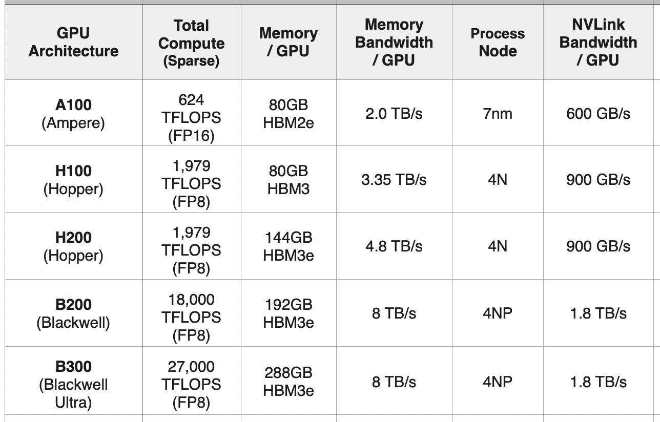
The Ampere Era (A100)
The A100 was the chip that industrialized deep learning. It introduced the third-generation Tensor Core—a specialized sub-unit inside the GPU designed specifically to accelerate dense matrix math.
It established HBM2e as the standard for memory, delivering 1.5 TB/s of bandwidth.
The A100 remains the backbone of many inference fleets today, but its lack of native FP8 support limits its efficiency for modern Large Language Models (LLMs).
The Hopper Era (H100 & H200)
With the H100, NVIDIA realized that AI models were becoming resilient enough to run on lower precision. They introduced the Transformer Engine, which dynamically adjusts calculations to 8-bit (FP8) precision.
Lower precision effectively doubled the throughput for LLMs without increasing the chip size. The H100 delivered 4,000 TFLOPS of FP8 compute (vs. ~600 TFLOPS of FP16 on the A100).
The Memory Upgrade: The H100 utilized HBM3 (3 TB/s bandwidth). Its mid-cycle refresh, the H200, upgraded this to 141 GB of HBM3e running at 4.8 TB/s, allowing larger models to fit on a single chip.
The Blackwell Era (B200)
Blackwell represents the current frontier. It is not just a bigger chip; it is a platform designed to be stitched together.
Precision: It introduces native FP4 (4-bit) support, doubling the raw throughput again to 9,000+ TFLOPS (FP4).
Bandwidth: It features 8 TB/s of memory bandwidth and 1.8 TB/s of NVLink interconnect speed, essential for the rack-scale architectures we will discuss later.
5. The Google TPU: The “Assembly Line” Machine
While NVIDIA GPUs dominate the merchant market, Google charted a different course starting in 2015. They realized that standard GPUs, carrying the legacy baggage of graphics rendering, were too inefficient for their scale.
The result is the Tensor Processing Unit (TPU)—an ASIC designed from the ground up for one specific workload: matrix multiplication.
The Heart of the TPU: The Systolic Array
The defining feature of the TPU is the Systolic Array.
How it works: In a standard GPU, data is constantly moved from memory to registers for every calculation. In a Systolic Array, data flows through a massive grid of processing units like a “heartbeat” (systole). The output of one unit flows directly into the input of the next without writing back to memory.
The Advantage: This drastically reduces register access and power consumption, making the TPU inherently more power-efficient per operation than a general-purpose GPU.
The Lineage of the TPU
Google’s silicon has evolved through three distinct eras, each solving a different bottleneck:
v1 (2015): The Inference Engine. A simple, air-cooled chip designed solely to run search queries and AlphaGo. It could run models, but it could not train them.
v2/v3 (2017-2018): The Training Pivot. Google added High Bandwidth Memory (HBM) and floating-point capability, allowing TPUs to train models. TPU v3 introduced liquid cooling to the data center years before it was common in the merchant market.
v4 (2021): The Optical Era. This generation introduced Optical Circuit Switches (OCS), allowing 4,096 chips to be connected in a reconfigurable 3D Torus mesh. This architecture defined the modern “Pod” structure that challenges NVIDIA’s clusters today.
TPU v5p (2023): Expanded the pod size to 8,960 chips, doubling the per-chip bandwidth to support larger models.
Google realized that “one size fits all” was inefficient, so they split their silicon strategy.
TPU v5e / Trillium (v6e): Designed for high-volume inference (Search, YouTube) where performance-per-dollar matters most.
TPU v7 “Ironwood”: A massive, high-density chip designed to for training and inference of frontier models like Gemini.
Here is the revised “Key Performance Definitions” section for Article 2. It now consistently uses the B200 and TPU v7 for every example to allow for a direct head-to-head comparison.
6. Conclusion
Both NVIDIA and Google have pushed their respective architectures—the flexible GPU and the efficient TPU—to the absolute limit of what a single piece of silicon can do.
In the next article, “Article 3: Two Strategies for Maximum Density,” we will look at how engineers are breaking this physical barrier—using 3nm process nodes, Chiplet packaging, and 4-bit precision to build the monsters that power the Gigawatt Machine.