
Two Strategies for Maximum Density
The Gigawatt Machine: NVIDIA, Google, and the Engineering of Scale 3/12

1. Introduction
In Article 1, we established that the “Gigawatt Machine” is defined by two competing architectural philosophies: NVIDIA’s hierarchical “Scale-Up” approach and Google’s flat “Scale-Out” approach.
These macroscopic architectures are not arbitrary; they are the direct expression of the microscopic silicon engines that power them. To understand why a data center looks the way it does, one must understand the limitations and capabilities of the processor at its core.
This article deconstructs the two primary engines of the AI era: the NVIDIA Blackwell B200 GPU and the Google TPU v7 “Ironwood.”
While both chips are Application-Specific Integrated Circuits (ASICs) designed for matrix multiplication, they represent divergent engineering paths.
2. The Physics of the Problem: Three Levers of Density
For decades, Moore’s Law allowed engineers to double performance simply by shrinking transistors. That era has ended. Modern photolithography has hit a hard physical barrier known as the “reticle limit”, the maximum size of a chip that can be etched in a single exposure (roughly 858 mm²).
Since engineers are nearing the limit of how many transistors they can squeeze on a chip, they have three remaining levers to increase performance:
The Process Lever (Transistor Density): The manufacturing process technology, measured in nanometers (nm). The “nm” label in a process node is shorthand for the generation of chipmaking technology. While historically it measured the physical size of a transistor, today it signifies a technology tier. Each step down the “node ladder” (e.g., 5nm —> 4nm —> 3nm) means increased compute density and higher performance.
The Packaging Lever (Silicon Area): Stitching multiple dies together to create a “Superchip” that physically exceeds the reticle limit.TSMC’s CoWoS (Chip-on-Wafer-on-Substrate) places multiple compute dies (GPU/TPU) and memory stacks (HBM) side-by-side on a massive silicon interposer, containing thousands of ultra-dense wires (far denser than standard circuit board).
The Precision Lever (Computational Density): Reducing the number of bits required for each calculation (e.g., 8-bit —> 4-bit). Traditional High-Performance Computing (like weather simulation) requires 64-bit precision. However, neural nets are more noise-resilient; distinguishing if next word is “the” or “cat” doesn’t require seven decimal places. The industry is moving to FP8 for training frontier models, while FP4 is being used for inference.
The Strategic Split:
In this generation, the two giants have pulled different levers.
NVIDIA paused the Process lever to go “all-in” on packaging and precision.
Google pulled the process lever.
3. The NVIDIA Strategy
NVIDIA’s Blackwell B200 represents a strategy of “architectural density.” Rather than moving to the 3nm process node, NVIDIA optimized the mature 4NP (4-nanometer) process to ensure high yields and reliability for a mass-market product.
The Dual-Die Design
The B200 is not a single chip.They manufactured two massive dies and stitched them together into a single GPU using advanced CoWoS-L packaging. This “chiplet” approach allowed them to pack 208 billion (vs. 80 Billion in Hopper)transistors into one unit. NVIDIA to effectively doubled the silicon area available for compute without the yield risks of a larger monolithic die.
The GB200 Superchip
NVIDIA’s packaging innovation extends beyond just making the GPU bigger. With the GB200 Grace Blackwell Superchip, they have fundamentally altered the definition of a “processor.”
The Innovation: Instead of plugging a GPU into a motherboard slot miles away (electronically speaking) from the CPU, NVIDIA packages two B200 GPUs and one Grace CPU onto a single board, fused by NVLink-C2C.
The Result: This is not just a “CPU next to a GPU”; it is a unified engine where the boundary between the two dissolves. By packaging them this tightly, NVIDIA eliminates the PCIe bottleneck entirely, allowing the GPUs to access the CPU’s massive LPDDR5X memory pool as their own.
The Precision Shift: FP4
The most significant leap in Blackwell is the sheer density of math operations it can perform.
H100 (Hopper): Delivered 4,000 TFLOPS of FP8 compute.
B200 (Blackwell): Doubles this to 8,000 TFLOPS of FP8 compute per GPU.
GB200 (Superchip): By fusing two B200s, the superchip delivers a staggering 16,000 TFLOPS of FP8 performance.
Crucially, the B200 architecture introduces native support for FP4 (4-bit Floating Point) precision. By processing data with half the bits of the previous generation, the chip can process twice as much data per clock cycle, doubling throughput again for inference workloads.
The Future of Density: Rubin and Rubin Ultra
NVIDIA’s ambition doesn’t stop at the chip. The goal is to make the “GPU” synonymous with the “Data Center.”
Today (Blackwell): The maximum size of a single NVLink domain is 72 GPUs (the GB200 NVL72). Beyond this, you must use a slower Tier-2 network.
Tomorrow (Rubin): With the upcoming Rubin (R100) architecture in 2026, NVIDIA plans to expand this domain to 144 GPUs.
The Horizon (Rubin Ultra): By 2027, the Rubin Ultra platform aims to connect 576 GPUs into a single, coherently addressed NVLink domain. This would effectively turn an entire aisle of racks into one massive, unified logic gate.
4. The Google Strategy
With the TPU v7 “Ironwood,” instead of relying solely on fabric scale, Google aggressively chased per-chip density by moving to TSMC’s cutting-edge 3nm (N3P) process. This allowed them to pack significantly more transistors into a single compute die (~700mm²) than was possible with 4nm technology.
The Economics of Yield: Why use a more expensive, lower-yield process than NVIDIA? Vertical Integration. Because Google does not sell the TPU chip (they sell the service), they can tolerate higher manufacturing costs and lower yields per wafer. They don’t need to protect hardware margins in the same way a merchant supplier like NVIDIA does.
Like Blackwell, the TPU v7 has moved beyond the monolithic die. It employs a dual-chiplet design, stitching together two massive compute dies and HBM memory stacks using advanced CoWoS packaging.
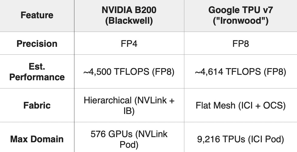
5. Head-to-Head: B200 vs. TPU v7
In an apples-to-apples comparison at FP8 precision, the two engines are remarkably close.
6. Conclusion
The B200 and TPU v7 represent two valid solutions to the end of Moore’s Law. While their per-chip performance is now effectively neck-and-neck (~4.6 PFLOPS), they differ radically in how they cluster that power.
At first glance, Google’s ability to connect 9,216 chips into a single domain seems vastly superior to NVIDIA’s limit of 72 GPUs (Blackwell) or 576 GPUs (Rubin Ultra). But this is not a case of “more is better”; it is a trade-off between Bandwidth Intensity and Fabric Extent.
NVIDIA: Scale Up
NVIDIA builds and connects ultra-dense islands.
The Domain: A single NVLink domain (72 or 576 GPUs) is a “tight” cluster. Inside this island, bandwidth is massive (1.8 TB/s per chip) and memory is fully unified. It is effectively one giant, coherently caching brain.
The Scale: To build a 100,000-chip supercomputer, NVIDIA connects ~1,400 of these islands together using InfiniBand.
The Advantage: This modularity allows for extreme flexibility. You can build a supercomputer of any size by simply adding more racks.
Google: Scale Out
Google builds massive, seamless meshes.
The Domain: A single TPU Pod (9,216 chips) is a “wide” cluster. The bandwidth per chip is lower (~1.2 TB/s), but the fabric extends much further without hitting a switch.
The Scale: To build a 100,000-chip supercomputer, Google connects ~11 of these massive pods together using Optical Circuit Switching.
The Advantage: This minimizes the “performance cliff” for massive models, as nearly the entire training run can stay within the optical fabric.
The Verdict:
They are neck-and-neck because they arrive at the same destination—the Gigawatt Machine—via different granularities.
NVIDIA stacks thousands of ultra-dense blocks.
Google weaves a few massive sheets.
Both architectures have successfully continued to scale even though the reticle limit has been reached.
But raw silicon power is useless without software to orchestrate it. In Article 4, “Two Software Foundations for Scale”, we examine how NVIDIA’s CUDA and Google’s XLA translate human intent into hardware action.
Great framing of how reticle limits are forcing divergent strategies. The part about NVIDIA's pause on process advancement to focus on packaging makes sense when you factor in the merchant silicon economics, they can't afford yield disasters at their volumes. What's intresting is how CoWoS becomes the real bottleneck going forward. Wether its Blackwell's dual-die or TPU's chiplet, everyone's waiting on TSMC's advanced packaging capacity now.